Circuit board design for the camera main logic board:
Given the specifications for the camera logic chip and the light sensor, I worked with other engineers to design and create the electrical schematic for the main logic board for the reference design camera.
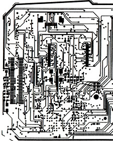
Then, I designed the physical circuit board, which involved working with a circuit-board layout technician who was an expert in specialized metalization-routing for the layers of the circuit board. His software would create a proposed routing of the connections needed, and then my job required scrutinizing this to look for trouble spots, for example, places where the software had routed connections in a way where there would be noise-contamination of the light signals from the digital imaging processing.
We designed multiple iterations of the circuit board to produce the best possible reference design for the camera. Here is an example showing a portion of just 1 of the 6 layers of circuit routing for this board: